v
vivekvellanki17

Electronics Eng

@vivekvellanki17

Specializing in KiCad routing schematics and IoT prototyping

India
Inglés, Telugu
Parte de la información aparece en idioma inglés.
Sobre mí
I am an Electronics and Communication Engineering student specializing in custom PCB layout design using KiCad. I focus on clean multi-layer trace routing, optimized power/ground planes, and rigorous Design Rule Checks (DRC) to minimize noise and manufacturing errors. With a live public portfolio on GitHub featuring functional hardware products, I deliver complete manufacturer packages including Gerber files, Drill logs, and Bill of Materials (BOM). Let's collaborate to bring your electronic hardware concepts to life!... Lee más

Habilidades

v
vivekvellanki17
Electronics Eng
desconectado • 
Tiempo medio de respuesta: 1 hora

Revisa mis servicios

Placas de circuito impreso (PCB)
I will design professional custom pcb layouts in kicad

Experiencia laboral

Self_employed / Freelance

Freelance PCB Designer

Self employed / Freelance • Freelance

Jun 2025 - Present1 yr 3 mos

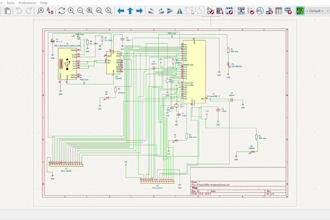
Designed custom 2-layer printed circuit boards (PCBs) and custom modules using KiCad. Successfully converted electronic schematics into production-ready layout traces, created custom component footprints, and performed full Design Rule Checks (DRC) to verify manufacturing compatibility. Generated manufacturing-ready Gerber outputs, drill logs, and complete Bill of Materials (BOM) packages for functional open-source hardware projects.