Explorar las categorías
Explora
Fiverr Pro
Español
$
USD
pcb design
HELLO GREAT BUYER
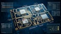
I'm a professional RF PCB Design Engineer with experience creating high-performance RF boards using Altium Designer, KiCad, and EasyEDA. I specialize in wireless communication hardware for IoT, embedded systems, industrial electronics, and custom RF applications.
What I Will Provide
RF Applications
Why Choose Me?
Let's Build Your RF Project!
Whether you're creating an IoT device, GPS tracker, LoRa node, GSM module, or another wireless product, I can deliver a reliable, production-ready RF PCB tailored to your requirements. Contact me today to discuss your project.


Especialización:
Diseño de circuitos
•
Esquemas
•
Disposición
•
Gerber
Formato de archivo:
Gerber
•
STEP
•
SCH
•
3DS
Software:
Eagle CAD
•
EasyEDA
•
KiCad
•
Matlab
•
Powersim
•
Proteus
Interfaz:
HDMI
•
I2S
•
Wi-Fi
•
BLE
•
BT
•
LTE
What do you need to get started?
Project requirements, schematic, RF frequency, PCB dimensions, layer count, BOM, antenna details, and reference files.
Can you design multilayer RF PCBs?
Yes. I design single, double, and multilayer RF PCBs with controlled impedance routing.
Can you review or improve an existing RF PCB?
Yes. I can optimize routing, signal integrity, grounding, and overall PCB performance.


