Explorar las categorías
Explora
Fiverr Pro
Español
$
USD
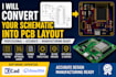
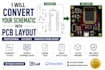
Embedded Systems and PCB Design Engineer
Welcome to my PCB Layout Gig!
Do you already have a schematic and need a professional PCB layout? I can convert your circuit diagram into a manufacturable PCB using KiCad and EasyEDA.
Services Included:
Applications:
Deliverables:
Please contact me before placing an order.
Especialización:
Esquemas
•
Disposición
•
Huella
•
Gerber
Formato de archivo:
Gerber
•
STEP
•
SCH
•
Software:
Altium Designer
•
EasyEDA
•
KiCad
•
Proteus
Interfaz:
UART
•
USB
•
SPI
•
I2C
•
Wi-Fi
•
Ethernet
What do you need to start?
Please provide schematic files, circuit diagrams, PDFs, images, or reference designs.
What files will I receive?
PCB source files, Gerber files, BOM, Pick & Place files, and 3D previews.
Can you create layouts for ESP32 and STM32 projects?
Yes
Do you support manufacturing?
Yes, I provide manufacturing-ready outputs.


