Explorar las categorías
Explora
Fiverr Pro
Español
$
USD
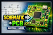
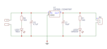
¿Tienes un esquema electrónico pero necesitas un diseño profesional de PCB?
Convertiré tu diagrama esquemático en un diseño de PCB de 2 capas limpio y fabricable usando EasyEDA.
Este servicio es perfecto para proyectos de hobby, placas Arduino, dispositivos IoT o electrónica personalizada que requiere un diseño de PCB confiable listo para fabricación.
Lo que haré
Lo que recibirás
Tu PCB estará lista para fabricar en servicios como JLCPCB o PCBWay.


Especialización:
Diseño de circuitos
•
Esquemas
•
Disposición
•
Gerber
Formato de archivo:
Gerber
•
Software:
EasyEDA
Interfaz:
Wi-Fi
Traducción automática
¿Qué archivos necesitas para comenzar el diseño de la PCB?
Por favor, envía tu diagrama esquemático, lista de componentes (si está disponible) y cualquier requisito de tamaño de placa.
¿Qué archivos recibiré?
Recibirás archivos Gerber, archivos de proyecto de EasyEDA y opcionalmente una Lista de Materiales (BOM).
¿El PCB está listo para fabricación?
Sí, la PCB será revisada con las reglas de diseño y preparada para servicios de fabricación como JLCPCB o PCBWay.


