o
otto_pcb1

Otto Markus

@otto_pcb1

High Performance PCB Layout! Circuit Design! Hardware Prototyping

Alemania
Alemán, Inglés, Francés, Chino, Español
Parte de la información aparece en idioma inglés.
Sobre mí
I’m Otto Markus, an experienced Electronics & PCB Design Engineer with 10+ years delivering high-quality schematic (Schaltplan) and PCB layout (Leiterplattenlayout) solutions. I specialize in EMV-optimized, production-ready (fertigungstauglich) designs using Altium Designer, KiCad, EasyEDA & Proteus. From simple circuits to complex embedded systems, I handle multilayer PCBs, high-speed routing, stack-up optimization, signal integrity, RF & power design, component selection (Bauteilauswahl), and firmware testing. Reliable, precise, and industry focused, built for serious projects.... Lee más

Habilidades

o
otto_pcb1
Otto Markus
desconectado • 

Revisa mis servicios

Placas de circuito impreso (PCB)
I will do custom pcb schematic design, pcb layout, with altium, kicad or easyeda
Placas de circuito impreso (PCB)
I will design power electronics pcb for inverter, smps, dc dc and motor drivers

Porfolio

Experiencia laboral

Electronicx

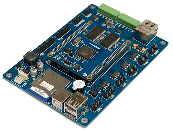
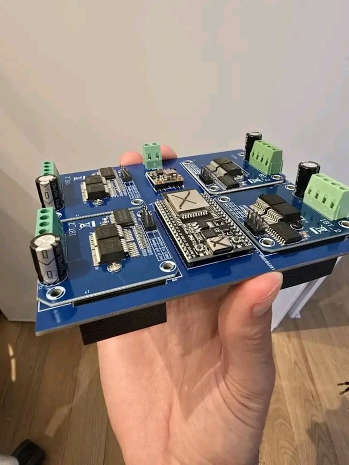
Senior PCB & Electronics Engineer

Electronicx • Freelance

Jan 2021 - Apr 20265 yrs 3 mos

I work as a freelance PCB and electronics engineer supporting startups and companies in Germany and the United States with multilayer PCB development for industrial, automotive, IoT, and medical applications. My work includes high-speed routing such as USB, Ethernet, DDR, CAN, and RF interfaces while applying signal integrity and EMI/EMC best practices. I regularly perform PCB redesign and troubleshooting of non-functional prototypes, develop stackup strategies with controlled impedance, and prepare full fabrication and assembly documentation including Gerber files, BOM, and Pick & Place data. I also conduct DFM and DFA validation in collaboration with PCB manufacturers and assembly partners.