m
mihikansha

Mihikansha

@mihikansha

PCB Design Engineer, PCB Layout and Electronics Design

India
Inglés, Hindi
Parte de la información aparece en idioma inglés.
Sobre mí
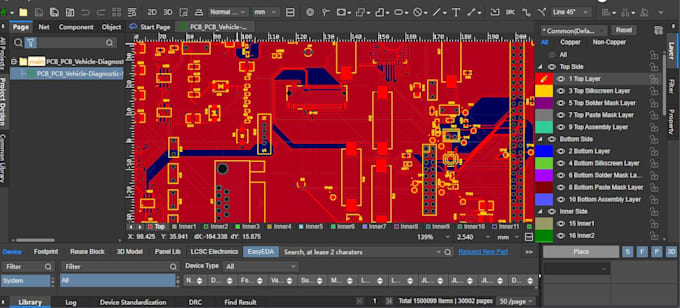
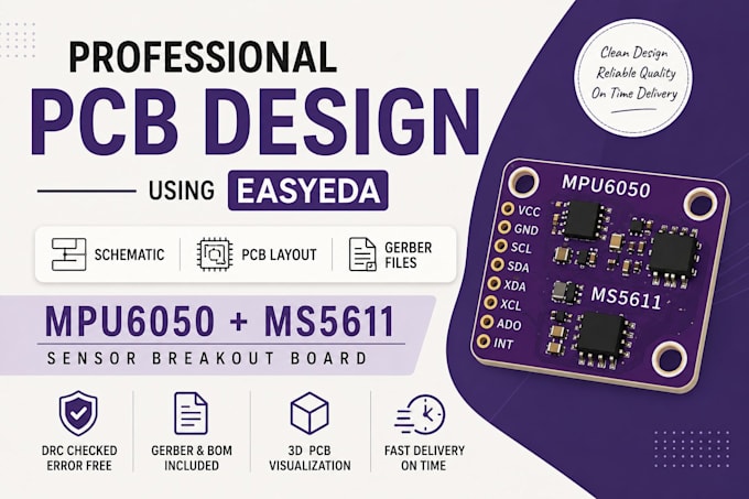
I specialize in PCB design using KiCad and EasyEDA. I can create schematics, PCB layouts, component placement, routing, and manufacturing-ready Gerber files. I focus on clean, reliable, and manufacturable PCB designs based on client requirements.... Lee más

Habilidades

m
mihikansha
Mihikansha
desconectado • 
Tiempo medio de respuesta: 1 hora

Revisa mis servicios

Placas de circuito impreso (PCB)
I will design pcb in kicad or easyeda

Experiencia laboral

Self_Employed

PCB Designer

Self Employed • Freelance

Aug 2026 - Present0 mos

I provide PCB design services using KiCad and EasyEDA, including schematic design, PCB layout, component placement, routing, design verification, and manufacturing-ready Gerber files. I focus on creating clean, reliable, and well-organized PCB designs based on client requirements.