Explorar las categorías
Explora
Fiverr Pro
Español
$
USD
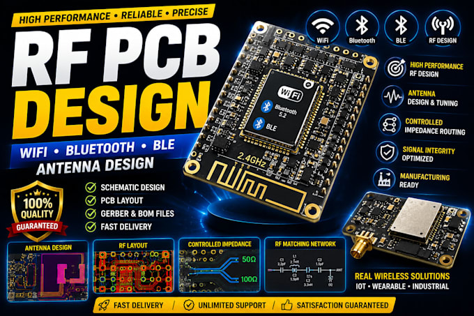
Architecture And PCB Design Engineer, Schematics, Technical Design
RF and wireless PCB design requires careful component placement, impedance control, antenna integration, and signal integrity considerations to ensure reliable real world performance.
I provide RF PCB design, WiFi and Bluetooth circuit development, ESP32 hardware deslgn, antenna integration, schematic capture, and manufacturing-ready PCB layouts for wireless and IoT applications.
Services Include
Whether you're developing a smart device, wireless sensor, industrial IoT product, BLE system, GPS tracker, automation controller, or custom embedded hardware, I can help transform your concept into a reliable and production-ready deslgn.
Kindly send a message with your project details so we can determine the most suitable solution for your wireless hardware requirements.