Explorar las categorías
Explora
Fiverr Pro
Español
$
USD

Junior KiCad PCB Layout and Schematic Entry Assistant
Habilidades
Revisa mis servicios

Freelance PCB Design & Hardware Engineer
Freelancing Career • Trabajador autónomo
Jun 2026 - Present • 1 mo
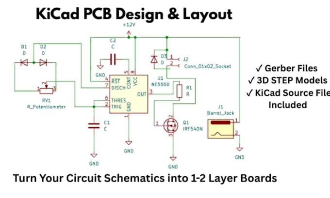
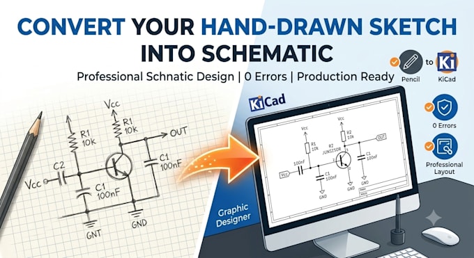
Independent Hardware Design Engineer specializing in end-to-end schematic capture, multilayer PCB layout optimization, and prototyping using KiCad. Deliver production-ready manufacturing packages with a strict focus on hardware reliability and zero design rule errors. Key Expertise & Services Offered: Schematic Capture & Optimization: Converting hand-drawn concept sketches, PDFs, or block diagrams into clean, industry-standard schematics. Multilayer PCB Layout: Routing high-density layouts, managing signal integrity, and integrating logic-level shifting for microcontrollers (Arduino, ESP32, STM32). Component Selection & BOM Optimization: Sourcing optimal components to reduce assembly costs while keeping performance high. DFM & Production Ready Packages: Generating comprehensive manufacturing deliverables including Gerber files (RS-274X/X2), Bill of Materials (BOM), and Centroid/Pick-and-Place files. Error-Free Execution: Ensuring 100% compliance with Design Rule Checks (DRC) and Electrical Rules Checks (ERC) before project delivery.
