Explorar las categorías
Explora
Fiverr Pro
Español
$
USD
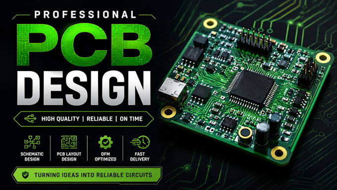
Experto en diseño de PCB y esquemas, soluciones IoT y circuitos
Cansado de las placas ESP32 que funcionan en breadboard pero fallan después de la fabricación? Soy Jan Lemann y diseño PCBs IoT que sobreviven en el mundo real, no solo en demostraciones de banco.
Tu producto IoT merece más que un kit de desarrollo apretado en una caja impresa en 3D. Me especializo en diseño de PCB multicapa con ESP32 y STM32, con enrutamiento RF WiFi/BLE, integración de sensores y distribuciones optimizadas para el consumo de energía.
Lo que obtienes:
Mi proceso:
Por qué elegirme:
Tus competidores ya están enviando productos. Contáctame ahora con tu lista de sensores y requisitos de energía. Responderé con un diagrama de bloques y una recomendación de distribución en capas en 12 horas. Vamos a sacar tu producto IoT del infierno del prototipo y a llevarlo a producción.
¡CONTÁCTAME AHORA!!!!
Traducción automática
¿Qué variante de ESP32 o STM32 debería usar?
Trabajo con ESP32-WROOM, WROVER, C3, S3, C6 y series STM32F1/F4/F7/H7. Durante nuestra llamada de requisitos, recomendaré el MCU óptimo según tus necesidades de WiFi/BLE, cantidad de GPIO, presupuesto de energía y objetivo de costo — luego optimizaré la colocación de antenas y el enrutamiento de memoria para esa variante específica.
Solo tengo una idea aproximada y sin esquema. ¿Aún puedes ayudarme?
Por supuesto. La mayoría de mis clientes comienzan solo con una lista de sensores y un boceto en una servilleta. Diseñaré el esquema completo desde cero, seleccionaré componentes con stock disponible y construiré la distribución del PCB — no necesitas archivos de diseño previos.
¿Cómo garantizas que mi placa funcionará después de la fabricación?
Tres capas de protección: (1) esquemáticos y distribuciones limpios en ERC/DRC antes de exportar, (2) validación DRC en JLCPCB/PCBWay para detectar problemas específicos de fabricación, (3) revisión de integridad de energía y señal para nets críticos. Mi tasa de éxito en el primer intento del 95% proviene de diseñar pensando en la manufacturabilidad, no solo en el diseño.
¿Puedes diseñar para IoT alimentado por batería con sueño profundo?
Sí, esa es mi especialidad. Optimizo rutas de energía, selecciono el LDO o convertidor buck adecuado, calculo presupuestos de corriente en modo sueño y apunto a menos de 100µA en sueño profundo cuando tu aplicación lo permite. Recibirás una hoja de cálculo de consumo de energía con la duración estimada de la batería antes de la fabricación.
¿Soy dueño de los archivos de diseño o están bloqueados a ti?
Eres dueño de todo. La opción premium incluye archivos fuente completos (.kicad_pcb, .sch, bibliotecas). Incluso los paquetes Básico/Estándar incluyen archivos Gerber y de fabricación que puedes llevar a cualquier fabricante. Sin bloqueo de proveedor, sin dependencias ocultas — tu propiedad intelectual permanece tuya.
