Hello,
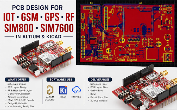
I'm Jack, a PCB Design Engineer with 5 years of experience in RF PCB, IoT, GSM GPS and wireless communication systems. I help with schematic design, multilayer PCB layout, RF routing and high speed PCB design for embedded and IoT applications. I use Altium Designer, KiCad and EasyEDA to create clean, reliable and production ready boards. My deliverables include schematic files, PCB layouts, Gerber files, BOM, Pick and Place files, 3D PCB renders and full manufacturing support for startups, businesses and hardware projects.... Lee más