Explorar las categorías
Explora
Fiverr Pro
Español
$
USD
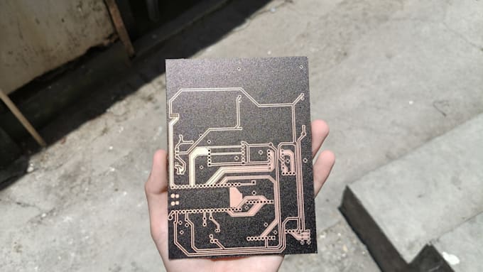
I design 2-layer boards for embedded systems, IoT devices, and custom electronics. I have hands-on experience with KiCad designing hardware. I design not just for routing, but also for signal integrity and real-world reliability.
WHAT YOU GET:


Especialización:
Diseño de circuitos
•
Esquemas
•
Disposición
•
Gerber
Formato de archivo:
Gerber
•
STEP
•
Software:
Otros
Interfaz:
I2S
•
UART
•
SPI
What if I don't have a schematic yet?
Please message me with a description of what your circuit does, and I can help you figure out the schematic before you order a gig
What if I need changes after delivery?
Offered packages have 1 to 2 revisions
Will my board actually work?
I check for common mistakes (floating pins, improper decoupling, trace width issues) and verify DFM before delivery. That said, I'm designing the layout—component selection and circuit design are your responsibility. Always prototype first.
Do you source components for me?
Unfortunately, the BOM I provide can only include part numbers. For sourcing, refer to your PCB manufacturer (JLCPCB, PCBWay), or to your component distributor (DigiKey, Mouser)