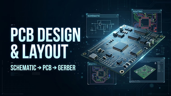
My work focuses on turning schematics and component information into organized PCB layouts with clean placement, routing, design-rule checks, and fabrication-ready documentation.
Services include PCB layout, component placement, signal routing, board organization, footprint setup, Gerber and drill file preparation, BOM organization, and editable project files where applicable.
I can work from an existing schematic, reference PCB, component list, or project requirements and help prepare the design for the next stage of prototyping or manufacturing.... Lee más