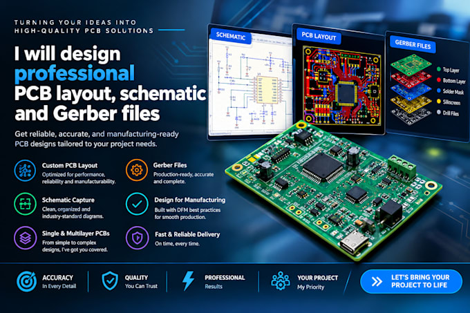
PCB Designer PCB Layout Schematic Design and Gerber Files
Estados Unidos
Inglés
Parte de la información aparece en idioma inglés.
Sobre mí
Hi! I am a PCB designer specializing in printed circuit board layout, schematic design, component placement, and routing. I help turn electronic ideas and circuit diagrams into organized, manufacturing-ready PCB designs.
My services include PCB layout design, schematic capture, component placement, PCB routing, Gerber file generation, drill files, and Bill of Materials (BOM) preparation.
Whether you need a new PCB layout, modifications to an existing design, or manufacturing files for your project, I am ready to help.... Lee más