d
david_rappaport

David Rappaport

@david_rappaport

Expert Schematic and PCB Design Engineer

Estados Unidos
Inglés, Francés, Alemán, Español
Parte de la información aparece en idioma inglés.
Sobre mí
PCB Design Expert specializing in professional schematic design, PCB layout, routing, and board optimization. I work with Altium Designer and KiCad to create reliable, production-ready PCB designs, including multi-layer, rigid-flex, RF, and embedded systems. I can handle projects from schematic reconstruction and component selection to layout, DRC validation, Gerber generation, BOM preparation, and manufacturing-ready source files. My focus is on accuracy, clean design, and practical engineering solutions.... Lee más

Habilidades

d
david_rappaport
David Rappaport
desconectado • 
Tiempo medio de respuesta: 1 hora

Revisa mis servicios

Placas de circuito impreso (PCB)
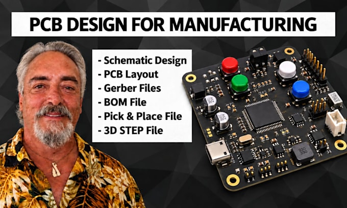
I will design circuit schematic and pcb layout ready for jlcpcb or pcbway manufacturing
Placas de circuito impreso (PCB)
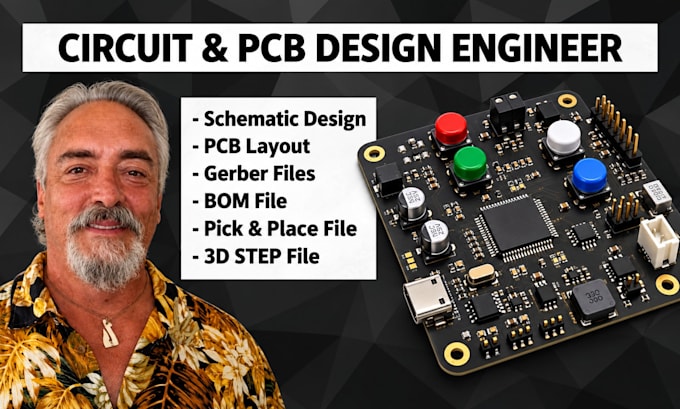
I will design circuit schematics and pcb layout in easyeda, altium or eagle kicad

Experiencia laboral

IOTA_Engineering

PCB Designer

IOTA Engineering • Tiempo completo

Aug 2015 - Present11 yrs 1 mo

I specialize in the use of Altium Design Tools V15,V16, V17 and have my own software license. I also have P-CAD, OrCad, and PADS software at my disposal. I have over 10 years of experience using Altium(23+ years designing PCB’s) and have successfully created designs of up to 26 layers incorporating mixed signal technologies, split plane architecture, high speed, matched length buses/differential pairs, DDR3 Ram, PCIe and USB 3.0 interfaces, switching and linear power supply architecture. I have also created and maintained numerous Design Libraries. I work with both Electrical and Mechanical Engineers to ensure that all designs meet both in-house and customer specifications