Explorar las categorías
Explora
Fiverr Pro
Español
$
USD
anu pcbdesigner
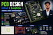
Welcome to my PCB design gig!
I will design professional, clean, and manufacturing-ready PCBs using KiCad for your electronics and embedded systems projects.
I can convert your idea, hand-drawn sketch, circuit diagram, or existing schematic into an organized PCB layout suitable for fabrication and assembly.
My services include:
PCB Design using KiCad
Schematic Design and Editing
Single-layer and Multi-layer PCB Layouts
Gerber File Generation
Bill of Materials (BOM)
Fabrication-Ready Files
3D PCB Preview
Component Placement and Trace Routing
Support for STM32, ESP32, Arduino, sensors, and communication interfaces such as UART, SPI, I2C, and USB
Why choose me?
Attention to detail
Clear communication throughout the project
Organized and professional deliverables
Timely delivery
Commitment to quality and continuous improvement
Please contact me before placing an order for complex designs so we can discuss your project requirements and choose the best package.
I look forward to helping bring your electronics and PCB design ideas to life.


Formato de archivo:
Gerber
•
STEP
•
SCH
•
3DS
•
Software:
EasyEDA
•
KiCad
Interfaz:
UART
•
USB
•
SPI
•
I2C
•
Wi-Fi
•
BLE


