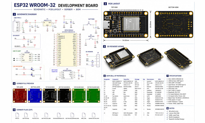
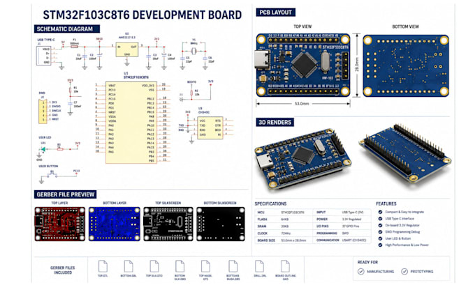
I am a professional PCB design engineer providing complete, production‑ready solutions from initial concept to final fabrication. I develop precise schematics, select optimized components, and design high‑performance multilayer layouts with controlled impedance, clean power distribution, and solid signal integrity. I deliver fully verified manufacturing packages including Gerbers, drill files, BOM, and pick‑and‑place data. I also audit and repair existing designs, correcting routing flaws, DRC violations, EMI risks, and manufacturability issues. ... Lee más